

A simple synchronizer comprises two flip-flops in series without any combinational circuitry between them. This design ensures that the first flip-flop exits its metastable state and its output settles before the second flip-flop samples it.You also need to place the flipflops close to each other to ensure the smallest possible clock skew between them.
Foundries help with signal synchronization by providing synchronizer cells. These cells usually comprise a flip-flop with a very high gain that uses more power and is larger than a standard flip-flop. Such a flip-flop has reduced setup-and hold- time requirements for the input signal and is resistant to oscillation when the input signal causes a metastable condition.
Another type of synchronizer cell contains two flip-flops, thus easing your job by placing the flip-flops close to each other and preventing you from placing any combinational logic between them. For synchronization to work properly, the signal crossing a clock domain should pass from flip-flop in the original clock domain to the first flip-flop of the synchronizer without passing through any combinational logic between the two (see Fig below).
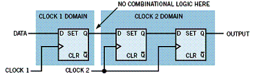 This requirement is important because the first stage of a synchronizer is sensitive to glitches that combination logic produces. A long enough glitch that occurs at the correct time could meet the setup-and-hold requirements of the first flip-flop in the synchronizer, leading the synchronizer to pass a false-valid indication to the rest of the logic in the new clock domain.
A synchronized signal is valid in the new clock domain after two clock edges. The signal delay is between one and two clock periods in the new clock domain.A rule of thumb is that a synchronizer circuit causes two clock cycles of delay in the new clock domain, and a designer needs to consider how synchronization delay impacts timing of signals crossing clock domains.
Synchronizers fall into one of three basic categories:
level, edge-detecting, and pulse.
Level Synchronizer:
In a level synchronizer, the signal crossing a clock domain stays high and stays low for more than two clock cycles in the new clock domain. A requirement of this circuit is that the signal needs to change to its invalid state before it can become valid again. Each time the signal goes valid, the receiving logic considers it a single event, no matter how long the signal remains valid. This circuit is the heart of all other synchronizers.
Edge Synchronizer:
The edge-detecting synchronizer circuit adds a flip-flop to the output of the level synchronizer (see Fig below). The output of the additional flip-flop is inverted and ANDed with the output of the level synchronizer. This circuit detects the rising edge of the input to the synchronizer and
generates a clockwide, active-high pulse. Switching the inverter on the AND gate inputs creates a synchronizer that detects the falling edge of the input signal. Changing the AND gate to a NAND gate results in a circuit that generates an active- low pulse.
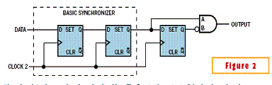 The edge-detecting synchronizer works well at synchronizing a pulse going to a faster clock domain. This circuit produces a pulse that indicates the rising or falling edge of the input signal. One restriction of this synchronizer is that the width of the input pulse must be greater than the period of the synchronizer clock plus the required hold time of the first synchronizer flip-flop. The safest pulse width is twice the synchronizer clock period. This synchronizer does not work if the input is a single clockwide pulse entering a slower clock domain; however, the pulse synchronizer solves this problem.
Pulse Synchronizer:
The input signal of a pulse synchronizer is a single clockwide pulse that triggers a toggle circuit in the originating clock domain (See Fig below). The output of the toggle circuit switches from high to low and vice versa each time it receives a pulse and passes through the level synchronizer
to arrive a
 t one input of the XOR gate, while a one-clock-cycle-delayed version goes to the other input of the XOR. For one clock cycle, each time the toggle circuit changes state, the output
of this synchronizer generates a single clockwide pulse.
The basic function of a pulse synchronizer is to take a single clockwide pulse from one clock domain and create a single clockwide pulse in the new domain. One restriction of a pulse synchronizer is that input pulses must have a minimum spacing between pulses equal to two synchronizer clock periods. If the input pulses are closer, the output pulses in the new clock domain are adjacent to each other, resulting in an output pulse that is wider than one clock cycle. This problem is more severe when the clock period of input pulse is greater than twice the synchronizer clock period. In this case, if the input pulses are too close, the synchronizer does not detect every one.

Your comments will be moderated before it appears here.