

Silicon testing covers every check a chip goes through from first silicon to shipment: wafer probe (sort), final test of packaged parts, burn-in, characterisation, qualification and silicon debug. Each stage catches a different kind of problem, from manufacturing defects to design bugs to early-life failures. Design for Test (DFT) is what makes these tests possible at a sensible cost, by building test access into the chip itself.
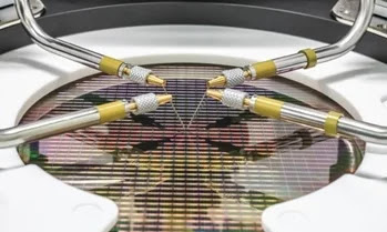
Picture courtesy: https://www.azom.com/
Key takeaways
- Testing happens at wafer level (probe or sort), at package level (final or class test), and in reliability and qualification flows.
- Production tests screen for manufacturing defects; characterisation and debug look at the design itself.
- Burn-in and qualification deal with reliability: early-life failures and long-term wear-out.
- DFT features such as scan, BIST, JTAG and test access mechanisms make high fault coverage possible in seconds of tester time.
- Test cost is driven by tester time, so DFT choices directly affect the cost of every chip shipped.
What is Design for Test (DFT)?
Silicon Design for Test (DFT) is a design methodology used in the development of integrated circuits. The goal of DFT is to make testing as efficient and effective as possible by designing chips with testability in mind. This includes inserting test circuits, providing access to internal signals and making other design changes so that the chip's functionality and performance are easier to test.
DFT techniques reduce the cost and time of testing by allowing more tests in a shorter time and by making it easier to identify and isolate defects. Without DFT, a tester could only drive the chip's pins and watch its outputs, and most internal flip-flops would be almost impossible to control or observe.
Key features of DFT
- Built-in self-test (BIST): BIST circuits are integrated into the chip to run internal tests and report results without needing external test equipment for pattern generation. Memory BIST (MBIST) for SRAMs and logic BIST (LBIST) are the common forms.
- Scan design: flip-flops are linked into shift registers (scan chains) so test patterns can be shifted into the chip's internal registers and results shifted out. This turns a hard sequential test problem into a much easier combinational one, and lets automatic test pattern generation (ATPG) tools create the patterns.
- Test access mechanisms (TAMs): TAMs carry test data to and from internal blocks and cores, making it easier to run tests and diagnose defects. Standards such as IEEE 1149.1 (JTAG boundary scan), IEEE 1500 (core test wrappers) and IEEE 1687 (access to embedded instruments) define common ways to do this.
- Reduction in test time: DFT reduces test time by enabling parallel testing of multiple blocks and by packing more tests into a shorter time. Scan compression is a major contributor, cutting the data and cycles needed per pattern.
By building DFT into a chip, designers improve the efficiency and effectiveness of testing, which helps ensure the chip meets its specifications and has a high level of reliability.
The different kinds of silicon testing
Here are the main types, roughly in the order a product meets them:
- Wafer probe testing: testing individual dies on a silicon wafer, using a probe card that touches the bond pads or bumps, to verify basic functionality and parametric performance before the wafer is diced.
- Class testing: the objective of class testing, as described in the original version of this post, is to verify the functionality and performance of individual components or blocks of the silicon, such as transistors, logic gates or memory cells. Note that in many companies "class test" is also the name used for package-level final test, so check how your organisation uses the term.
- Final testing (end-of-line test): testing packaged chips to verify performance and functionality under specified operating conditions, typically at one or more temperatures.
- Burn-in testing: high-stress testing of packaged chips, at raised voltage and temperature, to accelerate the detection of infant mortality failures before parts reach customers.
- Qualification testing: verifying that chips meet required reliability and environmental standards, for example the JEDEC reliability test methods or AEC-Q100 for automotive parts.
- Characterisation testing: measuring key parameters such as power consumption, speed and operating temperature range across many parts, voltages and temperatures, to set the data sheet limits and test limits.
- Production testing: ongoing testing of manufactured chips in volume to screen out defective parts and monitor performance and yield for any emerging issues.
- Silicon sort testing: separating good devices from bad ones based on their electrical characteristics. Sort is often the name for wafer-level production test, and parts may also be sorted into speed or power bins.
- Silicon debug: investigating first silicon and failing parts to find and fix design defects, using on-chip debug logic, scan dumps, failure analysis and lab equipment.
These tests are performed at various stages of development and manufacturing and help ensure that the devices meet their specifications and are functional and reliable.
How the stages fit together
| Stage | When | Main purpose | Typical content |
|---|---|---|---|
| Silicon debug and characterisation | First silicon, before volume | Find design bugs, set limits | Lab bring-up, shmoo plots, corner lots |
| Wafer probe or sort | Every wafer in production | Stop bad dies before packaging | Scan, MBIST, IDDQ, parametric checks |
| Burn-in | After packaging, product dependent | Screen early-life failures | Stress at raised voltage and temperature |
| Final or class test | Every packaged part | Confirm the shipped part works | Functional, at-speed, speed binning |
| Qualification | Once per product or process change | Prove long-term reliability | HTOL, temperature cycling, ESD, latch-up |
A worked example: why test time matters
The figures here are illustrative. Suppose a tester costs about 0.05 US dollars per second of use, including depreciation, handling and overhead, and a chip needs 4 seconds at wafer probe and 6 seconds at final test. Test then costs about 0.50 dollars per good part, before yield losses. If scan compression and better BIST cut the total to 6 seconds, the saving is about 0.20 dollars per part. At 10 million units a year that is roughly 2 million dollars, which is why test time is reviewed as carefully as die area.
Test quality is the other side. Fault coverage measures what fraction of modelled faults (for example stuck-at or transition faults) the patterns detect. Higher coverage lowers the number of defective parts that escape to customers, usually quoted in defective parts per million (DPPM). Automotive customers typically expect very low DPPM, which pushes coverage targets and adds tests such as burn-in.
Common mistakes
- Treating DFT as a late add-on: scan and BIST affect timing, area and power, so they belong in the plan from the architecture stage.
- Confusing verification with test: verification checks that the design is right before tape-out; manufacturing test checks that each chip was built right.
- Testing only at nominal conditions: some defects appear only at low voltage, high temperature or full speed.
- Ignoring diagnosis: patterns that detect faults but cannot help locate them make yield learning slow.
FAQ
What is the difference between wafer sort and final test?
Wafer sort tests bare dies on the wafer before packaging, so bad dies are not packaged. Final test checks each packaged part, including the effects of packaging, before it ships.
Is burn-in done on every chip?
Not always. It is common for high-reliability products such as automotive and server parts, and many consumer products reduce or skip it when the process is mature.
What does ATPG do?
Automatic test pattern generation tools create scan patterns that detect modelled faults and report the fault coverage achieved.
Is JTAG the same as scan?
No. JTAG (IEEE 1149.1) is a standard test access port and boundary scan architecture. Internal scan chains are often controlled through it but are a separate structure.
Each of these test types deserves a closer look, and we will cover them individually in upcoming posts.

Your comments will be moderated before it appears here.