
Gallium nitride (GaN) is a wide-bandgap compound semiconductor that has become a cornerstone of modern electronics, offering exceptional performance in high-power, high-frequency, and optoelectronic applications.
Its unique electrical and optical properties make it a game-changer in industries ranging from telecommunications to renewable energy and consumer electronics. GaN’s ability to handle high voltages, operate at high frequencies, and emit light efficiently has positioned it as a critical material for cutting-edge technologies.
This article delves into the history, properties, manufacturing processes, applications, advantages, challenges, and future prospects of gallium nitride, highlighting its transformative impact on the technological landscape.

History of Gallium Nitride
begins with the discovery of its constituent elements.
Gallium was identified in 1875 by French chemist Paul-Émile Lecoq de Boisbaudran, who named it after Gallia, the Latin name for France. Nitrogen, a well-known element, had been studied for centuries. The potential of combining these elements to form GaN was not explored until the 20th century.

In the 1930s, GaN was first synthesized, but early samples were of poor quality, limiting their practical use. Significant progress came in the 1960s when researchers at RCA Corporation, including Herbert Maruska and Jacques Pankove, used hydride vapor phase epitaxy (HVPE) to grow single-crystal GaN films in 1969. This work revealed GaN’s luminescent properties, sparking interest in its optoelectronic potential.
The 1980s and 1990s were transformative for GaN. Japanese researchers Isamu Akasaki, Hiroshi Amano, and Shuji Nakamura made groundbreaking advancements in growing high-quality GaN crystals using metal-organic chemical vapor deposition (MOCVD). Their work led to the development of the first practical blue light-emitting diode (LED) in 1993, a breakthrough that revolutionized lighting and display technologies. This achievement earned them the 2014 Nobel Prize in Physics. During this period, GaN’s potential for high-power and high-frequency electronics also gained attention, driven by its wide bandgap and robust properties.
By the 2000s, GaN began to enter commercial markets, with applications in LEDs, laser diodes, and power electronics. The development of GaN-on-silicon substrates in the 2010s significantly reduced costs, making GaN more accessible for consumer and industrial applications. Today, GaN is a key enabler of technologies like 5G networks, electric vehicle (EV) charging systems, and efficient lighting, with ongoing research pushing its boundaries further.
What is Gallium Nitride?
Gallium nitride is a III-V compound semiconductor, formed by combining gallium (Group III) and nitrogen (Group V) in a wurtzite crystal structure. As a wide-bandgap material with a bandgap of approximately 3.4 eV (compared to silicon’s 1.1 eV), GaN excels in high-performance applications requiring efficiency, speed, and durability.
Key Properties of GaN
- GaN’s 3.4 eV bandgap enables high-voltage and high-temperature operation, ideal for power electronics.
- With an electron mobility of ~2,000 cm²/V·s, GaN supports fast-switching devices for high-frequency applications.
- GaN can withstand electric fields up to 3.3 MV/cm, allowing for compact, high-power devices.
- GaN operates reliably at temperatures above 400°C, surpassing silicon’s thermal limits.
- GaN’s direct bandgap enables efficient photon emission, making it ideal for optoelectronic devices like LEDs and lasers.
These properties make GaN a superior alternative to silicon and a strong competitor to gallium arsenide (GaAs) in many applications.

Manufacturing Gallium Nitride
Producing high-quality GaN is a complex process, though advancements have improved its viability. The manufacturing process involves several key steps:
1. Raw Material Purification
Gallium is extracted from bauxite ore, while nitrogen is sourced from ammonia or other nitrogen-containing gases. Both require ultra-high purity (99.9999% or better) to ensure defect-free crystals.
2. Crystal Growth
GaN’s high melting point and nitrogen’s low solubility in gallium make crystal growth challenging. Common methods include:
Hydride Vapor Phase Epitaxy (HVPE): Used for growing thick GaN layers, often for substrates.
Metal-Organic Chemical Vapor Deposition (MOCVD): The primary method for depositing thin, high-quality GaN layers on substrates like sapphire, silicon, or silicon carbide (SiC).
Ammonothermal Growth: A newer technique for producing bulk GaN crystals, though it is slow and costly.

3. Substrate Challenges
Due to the high cost of native GaN substrates, GaN is typically grown on foreign substrates (heteroepitaxy) like sapphire, SiC, or silicon. GaN-on-silicon is increasingly popular for cost reduction, but lattice mismatch and thermal expansion differences can introduce defects.
4. Wafer Slicing and Polishing
Grown GaN crystals are sliced into thin wafers and polished to achieve a smooth surface for device fabrication.
5. Device Fabrication
GaN wafers undergo photolithography, etching, and doping to create devices like high electron mobility transistors (HEMTs), LEDs, and laser diodes. AlGaN/GaN heterostructures are commonly used in power and RF devices for enhanced performance.
GaN production remains more expensive than silicon due to substrate costs and complex growth processes, but GaN-on-silicon advancements are improving affordability.
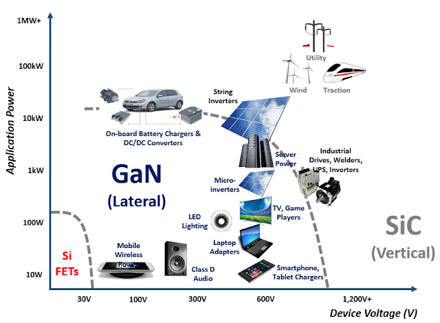
Applications of Gallium Nitride
GaN’s unique properties enable a wide range of high-performance applications.
1. Power Electronics
GaN’s high breakdown voltage and fast switching make it ideal for:
GaN-based inverters and chargers improve efficiency, reduce size, and enable faster charging.
GaN enhances efficiency in solar inverters and wind power systems.
GaN enables compact, high-efficiency power adapters for laptops, smartphones, and data centers.
2. Telecommunications
GaN’s high-frequency performance is critical for:
GaN power amplifiers support high-frequency, high-power 5G base stations, improving signal range and data rates.
GaN’s radiation resistance and high-frequency capabilities make it ideal for satellite RF systems.
3. Optoelectronics
GaN’s direct bandgap drives its use in:
GaN-based blue and white LEDs are used in lighting, automotive headlights, and displays for their efficiency and longevity.
GaN lasers power Blu-ray players, projectors, and medical devices.
GaN photodetectors are used in UV sensing for flame detection and sterilization.
4. Defense and Aerospace
GaN’s ruggedness supports:
GaN-based radar systems offer improved range and sensitivity.
GaN enables compact, high-power RF jammers and communication systems.
5. Consumer Electronics
GaN is used in fast chargers for smartphones and laptops, offering smaller, more efficient designs compared to silicon-based chargers.
Advantages of Gallium Nitride Over Silicon and GaAs
GaN offers several advantages over silicon and gallium arsenide:
- GaN’s wide bandgap reduces energy losses in power electronics, improving efficiency.
- Compact Designs:GaN’s high breakdown voltage enables smaller, lighter devices compared to silicon.
- GaN excels in RF applications, often outperforming GaAs in high-frequency, high-power scenarios.
- GaN’s high-temperature performance reduces cooling requirements.
- GaN’s direct bandgap supports UV and blue light applications, unlike silicon’s indirect bandgap.
Compared to GaAs, GaN offers higher voltage capabilities and better thermal stability, though GaAs may have an edge in specific high-frequency applications.
Challenges and Limitations
GaN faces several challenges:
- GaN substrates and manufacturing processes are expensive, particularly for native GaN wafers.
- Growing GaN on sapphire or silicon introduces defects, impacting performance.
- Substrates like sapphire have lower thermal conductivity, requiring careful design.
- MOCVD and other growth techniques require specialized equipment and expertise.
- Silicon’s mature ecosystem and economies of scale make it more cost-competitive for some applications.
The Future of Gallium Nitride
GaN is set to drive innovation in several fields:
- GaN’s high-frequency capabilities will support the ultra-fast, high-bandwidth demands of 6G networks.
- GaN will enhance efficiency in EV powertrains and grid-scale energy systems.
- GaN-based quantum dots are being explored for quantum computing and cryptography.
- GaN’s radiation resistance will support advanced electronics in space missions.
- Advances in GaN-on-silicon and ammonothermal growth will make GaN more affordable.
Research is focused on improving crystal quality, reducing defects, and scaling production. Recycling gallium from electronic waste could also address supply chain concerns.

Gallium nitride has evolved from a scientific curiosity to a pivotal material in modern technology. Its wide bandgap, high electron mobility, and thermal stability make it indispensable for power electronics, telecommunications, and optoelectronics.
From its early synthesis in the 1930s to its Nobel Prize-winning breakthroughs in the 1990s, GaN has transformed industries and continues to drive innovation. While challenges like cost and manufacturing complexity remain, ongoing advancements are making GaN more accessible. As we move toward a future of faster connectivity, sustainable energy, and advanced electronics, gallium nitride stands as a testament to the power of material science in shaping our world.