

A silicon interposer is a thin slice of silicon that acts as a high-density electrical bridge between multiple dies (chiplets) and the package substrate. It allows several semiconductor components to be connected using very short interconnects, fine-pitch routing, and extremely high bandwidth compared to a traditional printed circuit board (PCB) or organic substrate.
In simple terms, a silicon interposer is the “mini-silicon motherboard” sitting inside an advanced chip package. It routes signals between logic dies, high-bandwidth memory (HBM), I/O dies, and sometimes even integrates passive components.


Typical roles of the interposer include:
- Routing signals between logic chiplets, memory stacks (like HBM), and I/O dies
- Distributing power and enabling decoupling across the chiplet system
- Providing mechanical support for multi-die assemblies
- Enabling advanced packaging such as 2.5D (side-by-side dies) and 3D stacking
Because of these roles, silicon interposers are now a key enabler for high-performance computing (HPC), AI accelerators, networking ASICs, and next-generation data center SoCs.
Why Use a Silicon Interposer?
There are several strong motivations for using a silicon interposer:
1. Massive Bandwidth and Lower Latency
Interposers allow very short, dense interconnects between dies. This reduces signal latency and enables much higher bandwidth compared to traces on a PCB or traditional package substrate. You can route thousands of signals at fine pitch, which is exactly what AI GPUs and HBM memory stacks require.
2. Heterogeneous Integration & Chiplets
Instead of building one huge monolithic die, designers are moving toward chiplet architectures. Different functions (CPU, GPU, AI accelerator, I/O, analog, RF, memory, etc.) can be built as separate dies, often in different process nodes, and then placed on a silicon interposer. The interposer is effectively the high-speed “fabric” that ties all these chiplets together.
3. Thermal and Power Distribution Advantages
A silicon interposer enables better power distribution networks (PDNs) and allows decoupling capacitors to be placed very close to the chiplets. This improves power integrity and reduces noise. Thermal paths can also be more tightly controlled compared to long board-level traces.
4. Form Factor and System Integration
Interposer-based 2.5D/3D packaging allows far more compute and memory to be squeezed into a compact package. This is especially important in data centers, high-density servers, networking equipment, and compact AI appliances where board area is at a premium.
5. Yield and Manufacturing Flexibility
Large monolithic dies at advanced nodes can have yield challenges and high cost. With chiplets, each die can be smaller and manufactured on the most suitable process node. The interposer then brings them together. That can improve overall yield and reduce cost per functional system.
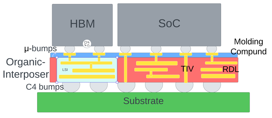
Anatomy of a Silicon Interposer Package


A typical silicon-interposer-based package consists of the following building blocks:
-
Silicon interposer wafer
A thin slice of silicon (often ~100–300 μm or more) processed with through-silicon vias (TSVs) or micro-vias, metal routing layers, and redistribution layers (RDL). These layers route signals between the top-side dies and the bottom-side package connections. -
TSVs (Through-Silicon Vias)
Vertical vias drilled and filled through the interposer that connect metal layers on the top and bottom. TSVs enable very short and dense vertical connections between the dies and the substrate. -
Micro-bumps / Flip-chip Interconnects
Logic or memory dies are flipped (face-down) and attached to the interposer using fine-pitch micro-bumps (often copper-based). Pitch can be in the 30–100 μm range, far denser than standard BGA packaging. -
Package substrate and solder balls (BGA)
The entire interposer + die assembly is mounted on an organic package substrate, which then connects to the PCB through solder balls or BGA. -
Routing layers / RDL
Fine-line copper routing on the interposer provides extremely dense wiring. These are fabricated using wafer-level lithography similar to front-end processes, but optimized for packaging. -
Passive device integration
Some interposers integrate passive components such as decoupling capacitors, resistors, or inductors directly into the silicon to further optimize signal integrity and power delivery.
2.5D vs 3D Integration – Where the Interposer Fits

2.5D Integration
In 2.5D integration, multiple dies are placed side-by-side on the interposer. The interposer itself lies between the dies and the package substrate. It provides high-density lateral routing between chiplets without the complexity of stacking dies directly on top of each other.
This approach is widely used today for GPU + HBM configurations, high-end FPGAs, and networking ASICs because it provides a good balance between performance, manufacturability, and cost.
3D Integration
In 3D integration, dies may be stacked vertically on top of each other, sometimes with a silicon interposer at the base. TSVs can pass through the dies and/or the interposer to provide vertical connections.
3D integration offers even higher integration density but brings significant challenges:
- More complex thermal management
- Increased stress and reliability concerns
- More challenging test flows and yield management
In industry usage, people often loosely refer to silicon-interposer-based solutions as “2.5D”, since they sit between conventional 2D and full 3D stacking.
Material and Manufacturing Considerations
While silicon interposers deliver excellent performance, they come with notable manufacturing and cost trade-offs. Some key aspects include:
Material Choices: Silicon, Glass, Organic
-
Silicon interposer
Best-in-class electrical and thermal performance, allows very fine-pitch routing, but is relatively expensive. -
Glass interposer
Emerging option with good dimensional stability and potentially lower cost for large formats, but still maturing. -
Organic interposer
Cheaper and easier to fabricate in large sizes, but with lower routing density and less favorable electrical characteristics compared to silicon.
Reticle Size Limits and Yield
Silicon interposers are typically fabricated using wafer lithography, which imposes a maximum reticle size (around 800–850 mm² for conventional 193 nm lithography). For very large interposers used in AI accelerators (multi-reticle), advanced stitching or other techniques are needed.
As the interposer size grows, the risk of defects and warpage increases, pushing down yield and driving up cost. This is one of the most important constraints for high-end silicon interposers.
CTE Mismatch and Reliability
The coefficient of thermal expansion (CTE) of silicon, organic substrates, and solder bumps differ. When the package heats and cools during operation, these mismatches can induce mechanical stress, leading to reliability concerns such as bump cracking or delamination.
Cost and Use-Case Selection
Due to all these factors, silicon interposers are generally reserved for high-value, performance-critical applications such as:
- AI accelerators (GPUs, NPUs)
- HPC CPUs and accelerators
- Network switches and routers at the highest speeds
- Advanced FPGAs
For mainstream or cost-sensitive applications, organic or hybrid interposer approaches may be more attractive.
Key Industry Use Cases & Company Highlights
TSMC – CoWoS®-S and CoWoS®-L
TSMC (Taiwan Semiconductor Manufacturing Company) is the clear market leader in silicon-interposer-based packaging with its CoWoS® (Chip on Wafer on Substrate) technologies.
- CoWoS-S: The classic silicon interposer-based implementation used in many AI and HPC products.
- CoWoS-L: A more recent variant that uses a local silicon bridge + RDL-based interposer concept to improve yield and enable larger packages at lower cost.
CoWoS-S is widely believed to be the technology behind AI giants like:
- NVIDIA’s H100, H200, and Blackwell accelerators
- AMD’s MI300 series
- Various custom AI ASICs from hyperscalers and networking vendors
TSMC is scaling interposer sizes from single-reticle to multi-reticle implementations, enabling packages with many HBM stacks and very large logic footprints. However, CoWoS capacity has become a bottleneck for the entire AI hardware ecosystem, highlighting how critical interposer-based packaging has become.
Xilinx (AMD) – Early Silicon Interposer Pioneer
Xilinx, now part of AMD, was one of the early adopters of silicon interposer technology in commercial products:
- The Virtex-7 2000T FPGA (announced around 2011) used a silicon interposer to combine four FPGA dies into one logical device, reaching about 6.8 billion transistors.
This was a landmark example showing that interposer-based multi-die integration could be productized at volume and used in real systems.
Intel – Foveros and Base-Tile Interposers
Intel has approached advanced packaging with a combination of technologies:
- EMIB (Embedded Multi-die Interconnect Bridge) – a small silicon bridge embedded in the organic substrate.
- Foveros – 3D stacking of chiplets with a base die acting somewhat like an interposer in certain implementations.
In platforms like Meteor Lake, Intel uses a base tile (in some ways interposer-like) to connect compute chiplets with TSV-based vertical connections and fine-pitch interconnects.
Packaging Specialists and New Players
Beyond the big foundries and IDMs, several packaging / OSAT companies are investing heavily in interposer and advanced packaging technologies:
- Powertech Technology Inc. (PTI) in Taiwan – working with AI chipmakers to provide packaging capacity comparable to CoWoS-style solutions.
- A new Japanese consortium of companies is exploring next-generation interposer manufacturing, including new materials and formats (such as square wafers and alternative substrates) to improve cost and scalability.
What’s Next for Silicon Interposers?
1. Scaling Interposer Size & Memory Integration
As AI models grow and GPUs demand more memory bandwidth, packages are evolving to support:
- More logic area (multiple GPU / accelerator chiplets)
- More HBM stacks (HBM3, HBM3E, HBM4)
This is driving interposer sizes toward multi-reticle designs, with roadmaps pointing to 5+ reticle-sized interposers and, in the longer term, even larger configurations. The challenge is to keep yield and cost under control as these structures become gigantic.
2. Hybrid Interposers: CoWoS-L and Beyond
Instead of a single huge monolithic silicon interposer, new approaches use:
- Local silicon regions only where very fine-pitch routing is needed
- Redistribution layers (RDL) on organic substrates elsewhere
This hybrid interposer concept helps reduce cost and improve yield, while still delivering high-bandwidth chiplet connectivity in critical areas. TSMC’s CoWoS-L and similar concepts from other vendors are good examples of this shift.
3. Open Chiplet Interfaces and Ecosystems
Standards such as UCIe (Universal Chiplet Interconnect Express) aim to enable interoperable chiplets from different vendors. This has far-reaching implications for how interposers are designed:
- Standardized SerDes or parallel interfaces on the interposer
- More modular chiplet-based system integration
If successful, this could turn interposers into standard multi-vendor chiplet backplanes, not just proprietary solutions.
4. Photonic & Optical Interposers
As electrical links hit limits in power and speed, researchers are exploring silicon photonics integrated on interposers. Optical links could enable:
- Ultra-high bandwidth between chiplets
- Lower power per bit
- Longer reach within packages and between packages
In the longer term, we may see photonic interposers that combine electrical and optical routing layers for truly bandwidth-unlimited systems.
5. Supply Chain & Capacity Challenges
The AI boom has exposed how constrained advanced packaging capacity can be. Foundries and OSATs are racing to expand:
- Interposer fab lines
- Micro-bump and assembly capacity
- Substrate and test infrastructure
This is not just a technology topic anymore – it’s a strategic supply chain challenge with national and corporate importance.
Design Challenges & Engineering Trade-Offs
Designing a silicon-interposer-based system is not just about “adding an extra layer under the dies.” It introduces new system-level challenges:
-
Interposer size vs. yield
Larger interposers are more likely to suffer defects and warpage. Designers must carefully partition the system across chiplets, decide how big the interposer must be, and balance cost and risk. -
Thermal management
Multiple chiplets on a single interposer can generate significant heat. Heat spreading, heat sink design, and thermal interface materials must be co-optimized with the interposer layout. -
Power delivery network (PDN)
The interposer must carry power to multiple dies with low IR drop and low noise. This often requires careful design of power/ground planes, TSV placement, and decoupling strategies. -
Routing congestion
HBM-based systems can require thousands of signals between logic and memory. Keeping routing clean, avoiding congestion, and managing timing is a non-trivial EDA challenge. -
Signal integrity and coupling
Even though interposer traces are short, crosstalk, return current paths, and simultaneous switching noise can still be problematic at multi-Gbps data rates. -
Test and yield management
Testing multi-die systems on an interposer is more complex. Known-good-die (KGD) strategies, boundary scan, and built-in self-test (BIST) become increasingly important.
Why This Matters to the India / Bengaluru Ecosystem
For design houses, startups, and engineering teams in India (and especially hubs like Bengaluru), silicon interposer technology opens several interesting opportunities:
-
Advanced SoC and chiplet design
As more companies move to chiplet-based architectures, there is demand for engineers who can co-design silicon and package – partitioning functions across dies, budgeting bandwidth, and designing die-to-die interfaces. -
EDA, design-automation and IP
Tool flows for 2.5D/3D ICs are still evolving. There is room for innovation in interposer-aware floorplanning, routing, power analysis, and package co-design, as well as reusable IP for die-to-die links. -
Packaging and OSAT ecosystem
While Taiwan and Korea dominate advanced packaging, there is a growing need for diversified capacity. India could develop niche capabilities in substrate design, test, and even advanced assembly over time. -
Materials and process R&D
Research into alternative interposer materials (e.g., glass, advanced organics) and improved TSV / RDL processes is an open field where academia and industry can collaborate. -
System-level innovation
For Indian OEMs and system integrators, interposer-based solutions make it possible to pack far more compute and memory into smaller edge devices, telco equipment, and AI appliances – all critical in a data-rich, bandwidth-hungry future.
Silicon interposers have quietly become one of the most important technologies in modern semiconductor packaging. They enable:
- High-bandwidth, low-latency connections between chiplets
- Integration of logic, memory, and heterogeneous functions in a single package
- New architectural possibilities for AI, HPC, networking, and more
At the same time, they introduce significant challenges in manufacturing, cost, yield, and supply chain. Companies like TSMC, NVIDIA, AMD, Intel, and leading OSATs are investing heavily to push interposer technology to new limits in size and complexity.
As the industry moves deeper into the chiplet era, understanding silicon interposers is no longer optional – it is becoming a core skill for anyone working in advanced semiconductors, whether you’re focused on architecture, design, packaging, or systems.

Your comments will be moderated before it appears here.