

Gallium nitride (GaN) is a wide-bandgap III-V compound semiconductor with a bandgap of about 3.4 eV, three times that of silicon. That wide bandgap gives it a breakdown field roughly ten times higher than silicon, and its AlGaN/GaN heterostructure forms a fast, high-density electron channel without doping. Together these let GaN transistors switch faster, at higher voltage and with lower losses than silicon in chargers, power supplies and RF amplifiers, while its direct bandgap makes it the material behind blue and white LEDs and blue-violet lasers.
GaN has become a cornerstone of modern electronics, from telecommunications to renewable energy and consumer products. This article covers its history, properties, manufacturing, applications, advantages, challenges and future prospects, with a worked example of why it allows smaller power devices.

Key takeaways
- GaN's bandgap is about 3.4 eV, against 1.12 eV for silicon; its critical breakdown field is about 3.3 MV/cm, roughly ten times silicon's.
- The two-dimensional electron gas (2DEG) at an AlGaN/GaN interface gives electron mobility of about 1,500 to 2,000 cm²/V·s, which is what makes GaN HEMTs fast.
- For the same voltage rating, a GaN drift region can be about ten times thinner than silicon's, so devices are smaller with lower capacitance and resistance.
- Most GaN power devices are grown on silicon wafers (GaN-on-Si); RF devices often use silicon carbide (GaN-on-SiC); LEDs mostly use sapphire.
- Cost, defects from foreign substrates, heat removal, and gallium supply concentration are the main challenges.
History of gallium nitride
The story of GaN begins with its elements. Gallium was identified in 1875 by the French chemist Paul-Émile Lecoq de Boisbaudran, who named it after Gallia, the Latin name for France. Nitrogen had been known for about a century. Combining the two to form GaN was not explored until the 20th century.

GaN was first synthesised in the 1930s, but early samples were poor powders of little practical use. Significant progress came in 1969, when Herbert Maruska and James Tietjen at RCA Laboratories, working in Jacques Pankove's group, used hydride vapour phase epitaxy (HVPE) to grow single-crystal GaN films on sapphire. This work revealed GaN's luminescent properties, and Pankove's team built early GaN light emitters in the early 1970s.
The 1980s and 1990s were transformative. Isamu Akasaki and Hiroshi Amano at Nagoya University grew high-quality GaN by metal-organic chemical vapour deposition (MOCVD) using a low-temperature buffer layer, and in 1989 achieved p-type GaN, which had long been the missing piece. Shuji Nakamura at Nichia developed his own growth process and, in 1993, announced a bright, practical InGaN blue LED, a breakthrough that changed lighting and displays. The three shared the 2014 Nobel Prize in Physics for efficient blue LEDs. In the same period, GaN's potential for high-power and high-frequency electronics also drew attention because of its wide bandgap and robust properties; the first AlGaN/GaN high electron mobility transistors were reported in the early 1990s.
By the 2000s, GaN had entered commercial markets in LEDs, laser diodes and RF power amplifiers. GaN-on-silicon substrates in the 2010s cut costs significantly, making GaN power devices practical for consumer and industrial use. Today GaN is a key enabler of 5G networks, compact chargers, data centre power supplies, electric vehicle (EV) charging systems and efficient lighting, with research still pushing its limits.
What is gallium nitride?
Gallium nitride is a III-V compound semiconductor formed from gallium (group III) and nitrogen (group V), usually in a hexagonal wurtzite crystal structure. As a wide-bandgap material with a bandgap of about 3.4 eV (compared with silicon's 1.1 eV), GaN excels in applications that need efficiency, speed and robustness.
Key properties of GaN
- Wide bandgap: 3.4 eV enables high-voltage and high-temperature operation, ideal for power electronics.
- High electron mobility: the original version of this post gave about 2,000 cm²/V·s. That figure applies to the 2DEG channel in AlGaN/GaN heterostructures (typically 1,500 to 2,000 cm²/V·s). Bulk GaN is lower, around 1,000 cm²/V·s. The 2DEG is what supports fast-switching devices for high-frequency applications.
- High breakdown field: GaN can withstand electric fields up to about 3.3 MV/cm, allowing compact, high-power devices.
- High temperature capability: the material itself remains a useful semiconductor at temperatures above 400°C, well beyond silicon's limits. Commercial GaN transistors are, however, typically rated for junction temperatures of about 150°C to 175°C because of packaging, gate and reliability limits.
- Direct bandgap: enables efficient light emission, making GaN ideal for LEDs and lasers.
- High saturation velocity: electrons in GaN reach about 2.5 x 10^7 cm/s, which helps RF performance.
These properties make GaN a strong alternative to silicon and a strong competitor to gallium arsenide (GaAs) in many applications.

How GaN compares with other semiconductors
Typical room-temperature values from textbook sources; exact numbers vary by source, doping and crystal quality.
| Property | Si | GaAs | 4H-SiC | GaN |
|---|---|---|---|---|
| Bandgap (eV) | 1.12 | 1.42 | 3.26 | 3.4 |
| Bandgap type | Indirect | Direct | Indirect | Direct |
| Critical field (MV/cm) | about 0.3 | about 0.4 | about 2.5 to 3 | about 3.3 |
| Electron mobility (cm²/V·s) | about 1,400 | about 8,500 | about 900 | about 1,000 bulk, 1,500 to 2,000 in a 2DEG |
| Thermal conductivity (W/cm·K) | about 1.5 | about 0.5 | about 3.7 to 4.9 | about 1.3 to 2.3 |
How a GaN transistor works
Most GaN power and RF transistors are high electron mobility transistors (HEMTs). A thin layer of aluminium gallium nitride (AlGaN) is grown on GaN. Because both materials are strongly polar and their lattices differ slightly, built-in polarisation charges form at the interface and pull electrons into a sheet only a few nanometres thick. This two-dimensional electron gas has a typical density of about 10^13 electrons per cm² and high mobility, without any intentional doping.
The 2DEG is present with no gate voltage, so a basic HEMT is "normally on" (depletion mode). Power converters need devices that are off when undriven, so manufacturers use either a p-GaN gate layer that removes the 2DEG under the gate (enhancement mode) or a cascode, pairing a depletion-mode GaN HEMT with a low-voltage silicon MOSFET.
Worked example: why GaN devices are smaller
A simple estimate, assuming a triangular field profile in a one-sided junction, gives the drift region thickness needed to block a voltage V as about W = 2V / Ec. For a 650 V device (illustrative, ignoring safety margins):
- Silicon, Ec about 0.3 MV/cm: W = 1,300 V / 300,000 V/cm = 43 µm.
- GaN, Ec about 3.3 MV/cm: W = 1,300 V / 3,300,000 V/cm = 3.9 µm.
The GaN drift region is about eleven times thinner and can also carry far more charge per unit area. Combined, these give much lower on-resistance for a given die area. The commonly used Baliga figure of merit, which scales with permittivity, mobility and the cube of critical field, comes out several hundred times higher for GaN than silicon. Smaller dies have smaller capacitances, which is why GaN switches fast with low switching loss, and why GaN chargers can run at higher frequency with smaller magnetics.
Manufacturing gallium nitride
Producing high-quality GaN is complex, though advances have improved its viability. The main steps are:
1. Raw material purification
Gallium is recovered mainly as a by-product of alumina production from bauxite ore, and to a lesser extent from zinc processing. For growth, nitrogen comes from ammonia or other nitrogen-containing gases, and gallium from metal-organic precursors such as trimethylgallium. Both need ultra-high purity (99.9999% or better) for low-defect crystals.
2. Crystal growth
GaN's very high melting point and the low solubility of nitrogen in liquid gallium make bulk crystal growth difficult. Common methods include:
- Hydride vapour phase epitaxy (HVPE): used for growing thick GaN layers, often to make free-standing GaN substrates.
- Metal-organic chemical vapour deposition (MOCVD): the main method for depositing thin, high-quality GaN and AlGaN layers on substrates such as sapphire, silicon or silicon carbide (SiC).
- Ammonothermal growth: a newer technique for producing bulk GaN crystals; it gives very high quality but is slow and costly.

3. Substrate challenges
Because native GaN substrates are expensive, GaN is usually grown on foreign substrates (heteroepitaxy) such as sapphire, SiC or silicon. GaN-on-silicon is increasingly popular for cost reduction and because it can use existing silicon fabs, but the lattice mismatch (about 17% to silicon) and thermal expansion differences introduce defects and wafer bow, which buffer layers must manage.
4. Wafer slicing and polishing
Bulk GaN crystals are sliced into thin wafers and polished to a smooth surface for device fabrication. For GaN-on-silicon and GaN-on-SiC, the foreign substrate is the wafer, and the GaN is grown on it as an epitaxial layer only a few micrometres thick.
5. Device fabrication
GaN wafers then go through photolithography, etching, doping or implantation for isolation, and metallisation to create HEMTs, LEDs and laser diodes. AlGaN/GaN heterostructures are commonly used in power and RF devices for better performance.
GaN production remains more expensive than silicon because of substrate costs and complex growth, but GaN-on-silicon progress, including the move to 200 mm and, as Infineon announced in 2024, 300 mm wafers, is improving affordability.
Applications of gallium nitride
GaN's properties enable a wide range of high-performance applications.
1. Power electronics
GaN's high breakdown field and fast switching make it ideal for:
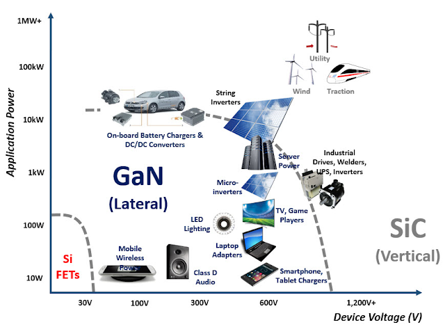
- Electric vehicles: GaN inverters and chargers improve efficiency, reduce size and enable faster charging. Today GaN is used mainly in on-board chargers and DC-DC converters; most traction inverters still use SiC or silicon IGBTs, though GaN traction inverters are being developed.
- Renewable energy: GaN improves efficiency in solar inverters and other energy conversion systems.
- Power supplies: GaN enables compact, efficient power adapters for laptops and smartphones, and high-efficiency server power supplies for data centres.
2. Telecommunications
GaN's high-frequency performance is critical for:
- 5G infrastructure: GaN power amplifiers support high-frequency, high-power 5G base stations, improving range and data rates.
- Satellite communications: GaN's radiation tolerance and high-frequency capability suit satellite RF systems.
3. Optoelectronics
GaN's direct bandgap drives its use in:
- LEDs: GaN-based blue LEDs, and white LEDs made from blue LEDs with a phosphor, are used in lighting, automotive headlights and displays for their efficiency and long life.
- Laser diodes: 405 nm GaN lasers power Blu-ray players, and GaN lasers are used in projectors and medical devices.
- UV photodetectors: GaN and AlGaN detectors are used for UV sensing in flame detection and sterilisation.
4. Defence and aerospace
GaN's ruggedness supports:
- Radar: GaN-based radar systems offer improved range and sensitivity.
- Electronic warfare: GaN enables compact, high-power RF jammers and communication systems.
5. Consumer electronics
GaN is used in fast chargers for smartphones and laptops, giving smaller, more efficient designs than silicon-based chargers.
Advantages of gallium nitride over silicon and GaAs
- Higher efficiency: low on-resistance and fast switching reduce energy losses in power electronics.
- Compact designs: the high breakdown field allows smaller, lighter devices than silicon, and higher switching frequency shrinks magnetics.
- High-frequency performance: GaN excels in RF, often outperforming GaAs in high-frequency, high-power applications.
- Thermal robustness: high-temperature capability reduces cooling requirements.
- Optoelectronic versatility: GaN's direct bandgap supports UV, blue and green light emission, unlike silicon's indirect bandgap.
Compared with GaAs, GaN offers higher voltage capability and better thermal stability, although GaAs can still have the edge in specific applications, such as low-voltage, low-noise or mobile handset amplifiers.
Challenges and limitations
- High cost: GaN substrates and manufacturing processes are expensive, especially native GaN wafers.
- Defects: growing GaN on sapphire or silicon introduces dislocations that affect performance and reliability.
- Thermal management: substrates such as sapphire have low thermal conductivity, and high power density in small dies needs careful thermal design.
- Manufacturing complexity: MOCVD and other growth techniques need specialised equipment and expertise.
- Competition from silicon: silicon's mature ecosystem and economies of scale keep it more cost-competitive for many applications.
- Device-level issues: dynamic on-resistance (current collapse from charge trapping), gate reliability and the lack of avalanche capability need careful qualification.
- Supply concentration: most of the world's primary gallium is produced in China, which introduced export licensing for gallium in August 2023 and tightened controls further in late 2024.
The future of gallium nitride
- 6G: GaN's high-frequency capability will support the high-bandwidth demands of future 6G networks.
- Electric vehicles and grid systems: GaN will improve efficiency in EV power electronics and energy systems.
- Quantum technologies: GaN-based quantum dots are being explored as single-photon sources for quantum communication and cryptography, and possibly for quantum computing.
- Space: GaN's radiation tolerance will support electronics for space missions.
- Cost reduction: advances in GaN-on-silicon, larger wafers and ammonothermal growth will make GaN more affordable.
- Integration: monolithic GaN power ICs that combine the switch, driver and protection on one die are spreading.
Research focuses on better crystal quality, fewer defects and larger-scale production. Recycling gallium from electronic waste could also ease supply chain concerns.

Common misconceptions
- "GaN will replace SiC." They overlap at 650 V, but SiC dominates high-voltage, high-current uses such as EV traction inverters, and GaN leads at lower voltages and higher frequencies.
- "GaN runs hotter, so it is less reliable." GaN dies are smaller and run at high power density, but their losses are lower; reliability depends on qualification, not on the material alone.
- "GaN is a new material." It has been in volume production in LEDs since the 1990s; what is newer is its use in mainstream power electronics.
Conclusion
Gallium nitride has gone from scientific curiosity to an essential material in modern technology. Its wide bandgap, high electron mobility in heterostructures and thermal robustness make it indispensable for power electronics, telecommunications and optoelectronics. From its first synthesis in the 1930s to the Nobel Prize-winning breakthroughs of the late 1980s and 1990s, GaN has transformed industries and continues to drive innovation. Cost and manufacturing complexity remain real challenges, but steady advances are making GaN more accessible for faster connectivity, cleaner energy and advanced electronics.
FAQ
Why is GaN called a wide-bandgap semiconductor?
Its bandgap of about 3.4 eV is much larger than silicon's 1.12 eV. Materials above roughly 2 to 3 eV, such as GaN and SiC, are usually grouped as wide-bandgap semiconductors.
What is the difference between GaN and SiC for power?
Both are wide-bandgap. GaN switches faster and suits roughly 100 V to 650 V converters at high frequency; SiC handles higher voltages (1,200 V and above) and currents with better thermal conductivity.
Why are GaN chargers smaller?
GaN transistors have low switching losses, so the charger can run at a higher frequency. Higher frequency allows smaller transformers and capacitors, which take most of the space.
What is GaN-on-Si?
GaN epitaxial layers grown on standard silicon wafers. It is cheaper than native GaN or SiC substrates and can use silicon fab equipment, which is why most GaN power devices use it.

Your comments will be moderated before it appears here.